Table Of Content
How do you go about taking your great idea and turning it into a real design, and eventually into a finished product? Any new circuit board can be very complicated, but the right PCB design process methodology helps you get through the design process quickly. There are multiple additional aids available to the designer, such as design grids that can help to place components and route traces in a neat and orderly manner. Although the design and manufacturing of a PCB can be generalized as schematic capture, PCB layout, and circuit board fabrication and assembly, the details of each step are very involved. We’ll take a look here at some of the more specific aspects of each of these steps. Once the schematic sets the stage, the next step in the journey of creating a Printed Circuit Board (PCB) is to simulate the circuitry.
Best PCB Design Software – Full Round-Up
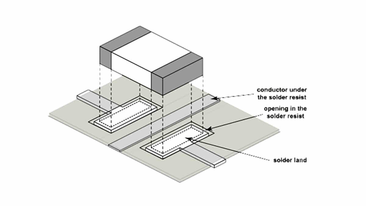
The width of the traces and the spacing between them are critical for maintaining the required impedance and preventing signal degradation. Consult the design guidelines provided by your PCB manufacturer to determine the appropriate trace widths and spacing for your design. While they are necessary, excessive use of vias can increase the complexity of the design and affect signal integrity.
IPC Board Design Standards
The common material for these boards is FR-4, but depending on the particular needs of the design, this can be modified to emphasize or otherwise improve certain characteristics of the board. These ICs are usually smaller than the microcontrollers, or other ICs on a circuit board, with pin counts in the three to twenty range. DIP sensor ICs are becoming a rarity, as modern components are usually found in QFP, QFN, even BGA packages. Simple microcontrollers can be found in packages ranging from DIP to QFN/QFP, with pin counts lying somewhere between eight and a hundred.
Step 3: PCB Design – Your Board Layout
Some of our products- LilyPad boards and Arudino Pro Micro boards- use a 0.8mm thick board. I typically recommend using copper pour on both sides to provide the remaining ground connections and shielding unless there is some reason to omit this. PSI’s award-winning Repairable Asset Control (RAC®) service offers on-site management of MRO parts and manufacture of obsolete/legacy components.
Not only is circuit interconnectivity easier to define and edit, but converting a schematic to a circuit board layout is much easier than designing directly on the board. For components, Altium Designer has an extensive database of parts libraries. Additionally, you can utilize the Altium Vault, which provides access to thousands of component libraries and adds flexibility to your project management and product development. However, you can also design your own schematic symbols and create footprints.
What Is a Printed Circuit Board?
The integrated LibrePCB Fab service also allows for easy PCB ordering through Aisler with a portion of profits fed back into the development of the program. A unified PCB design package with the best tools for implementing the right PCB design process methodology for your next circuit board. When designing a printed circuit board (PCB), one of the critical factors to consider is the return current path. The return current path refers to the path that the current takes to complete the circuit and return to its source.
This version is compatible with Xpedition technology and is designed to support the entire design and verification pipelines for PCB and hardware engineers, while also providing additional collaborative features. It boasts the same intuitive interface and sleek design as Altium’s professional solutions, making it one of the best PCB software for beginners and hobbyists. It allows you to design with up to 16 signal and 16 plane layers, with no limits on dimensions. Altium provides a truly unified, photorealistic 3D design environment, with a single view of every step of the PCB design process. Having all the design tools and documentation across one intuitive platform really helps to streamline your design workflow. The industry's best ECAD software should be easy to use and easy to learn, and it should include a complete set of design features.
Design process

These PCB board design guidelines only scratch the surface, but they form a foundation for building upon and solidifying a practice of continual improvement in all your design practices. In many layouts, you'll have some analog and some digital components, and you should prevent the digital components from interfering with the analog components. The way this was done decades ago was to split up ground and power planes into different regions, but this is not a valid design choice in modern board designs.
Eagle is a fairly straightforward tool that has all the features you need to make PCB designs. The schematic editor has a SPICE simulator that allows you to quickly test ideas, as well as electronic rule checks to validate circuit performance. The modular design blocks use a simple drag-and-drop method that you can use to add blocks to different projects. Designed by Novarm, DipTrace aims to bring full PCB design options and functionality while keeping the experience simple and intuitive. Foundries supply libraries of standard cells to fabless companies, for design purposes and to allow manufacturing of their designs using the foundry's facilities. Macros/Macrocells/Macro blocks,[7] Macrocell arrays and IP blocks have greater functionality than standard cells, and are used similarly.
Attend the expertly curated 14-track conference created by engineers for engineers featuring technical paper sessions, tutorials, and industry panels covering all aspects of chip, board, and systems design. If you need a PCB design tutorial to help you get up to speed quickly, you’ll have access to a variety of resources you need to be successful. The resources listed below contain PCB routing tutorials, guides on how to use PCB design tools, and much more. Anyone can access Altium’s knowledge base, blogs, webinars, and more for free. Visualization tools help users check component information and manage BOM in real-time.
Wherever controlled electromagnetism exists, printed circuit boards form the infrastructure to maintain it. Of course, circuit boards don’t just spring out from nothingness–their design and manufacturing are a huge engineering undertaking unto themselves. To design and create PCBs, engineers and designers rely on Computer-Aided Design (CAD) tools. Before diving into the setup process, it's important to choose the right CAD tool for your PCB design needs.
Plus, any designs released to the community can be reused as base templates and then modified, so you don’t need to start from scratch for every project. There’s also a non-profit version that’s 100% free but limited to 500 pins and 2 signal layers, rising to $350 for unlimited functionality. For the full fat version for commercial use with unlimited pins and signal layers, expect to pay around $1000. DipTrace is license based with quite a few buying options, the cheapest of which is the DipTrace starter at $75, which include 300 pins and 2 signal layers. Students and educational institutions can get DipTrace Lite (capped at 500 pins and 2 signal layers) for free.